What is Automated Optical Inspection (AOI) in a PCB?
Automated Optical Inspection (AOI) is an extremely useful tech used in PCB fabrication to detect various defects for quality control. Quality control in manufacturing is crucial to ensure that products are free from defects and meet customers’ expectations. Read on to learn about AOI, when to apply it, what defects it can detect, its benefits, and more.
What is AOI, and When to Apply it in Detecting the PCB?
Automated Optical Inspection is a machine vision technology used during manufacturing to inspect products for defects. An AOI system consists of an illumination system, a computer system, and a camera system. The illumination system uses light from one or more directions to illuminate the PCB assembly. The camera captures images of the assembly from various angles. The computer analyzes those images to find defects.
AOI is useful at various stages of production. It is applicable for pre-reflow Inspection, bare board inspection, solder paste inspection, and post-reflow Inspection. Since any of these stages can introduce defects in the PCB design, the use of AOI proves to be invaluable here.
What Can the AOI Detect?
There are two primary types of PCB failures/defects that automated optical Inspection can detect. These include the following:
1. Soldering Defects
Metal components of a PCB are connected via soldering. Many soldering defects may occur and should be identified on time. AOI detects the following defects:
- Insufficient Solder:Insufficient solder can severely affect the board’s performance as the components are not properly connected.
- Excess Solder:Using excess solder can result in problems like short circuits.
- Open Circuits:When the pad and the lead have a broken connection or no connection, this defect occurs. Open circuits are difficult to detect unless you use automated optical Inspection.
- Solder Shorts:Solder shorts occur when the solder connects two or more PCB components that should be solder-free. The human eye cannot detect this defect, but AOI can.
2. Component Defects
Component defects are defects that occur in the small functional parts that are attached to the PCB board. Automated optical Inspection can detect the following component defects:
- Misaligned or Misplaced Component:This defect can severely affect the performance of the board.
- Lifted Lead:This defect occurs when small metal pads of the PCB fail to stick correctly. Other causes include excessive heat, improper handling during production, etc.
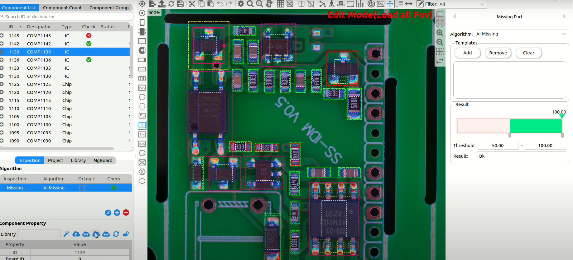
- Missing Components:This common defect often occurs due to inadequate soldering.
Advantages of Automated Optical Inspection
SMT 2D AOI with one-click search&repeat PCB to achieve fast programming
Automated optical Inspection has many key advantages. It provides more reliable, faster examination and ensures quality control in PCAB tests and fabrication. Here are some of its top benefits:
- Ensuring Quality
Automated optical Inspection can detect defects in electronic PCBs, components, and assemblies with great accuracy and helps ensure that only the best quality products reach customers.
- Improving Process
Automated optical Inspection facilitates high-speed production and high-volume manufacturing. It improves production efficiency and allows for continuous process improvement.
- Customizability
AOI is highly customizable. You can configure the inspection parameters for faster, more efficient scanning and Inspection.
Consider Dependable AOI Products from Maker-ray
AOI products offer many advantages, making them a valuable investment for quality control in PCB fabrication. However, not all AOI products are created equal. For the best results, buying from a reputed supplier is crucial. Maker-ray is a seasoned high-tech manufacturer of intelligent optical inspection products and solutions that offers a wide range of products to cover various applications.
At Maker-ray, we focus on offering optical inspection products that deliver consistent performance, accurate results, and fast problem-solving capabilities. Our products cover five different fields, i.e.:
- SMT 2D/3D AOI
- SPI 3D
- THT AOI /final inspection
- Coating AOI
- Semiconductor (MLED) Inspection
All of our products are AI-powered. We develop AOI solutions that feature deep learning algorithms, one-click automatic identification of solder and components, minimalist intelligent programming, and more. Our products have a low false positive rate and intelligent judgment of defectiveness. These characteristics make them an attractive choice for most consumers.
Conclusion

The demand for automated optical Inspection in PCB fabrication is increasing, and the technology these products feature continues to improve. AOI products and solutions from Maker-ray feature increased throughput, enhanced speed and accuracy, customizability, and more.
Maker-ray is a brand with a reputation for excellence. We are at the forefront of providing intelligent optical inspection products suitable for a wide range of applications. Our commitment to quality, attention to detail, and focus on the latest technologies make us one of the top brands in the industry. Visit our website to learn more about our automated optical inspection products.