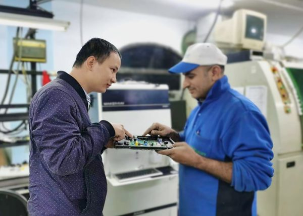
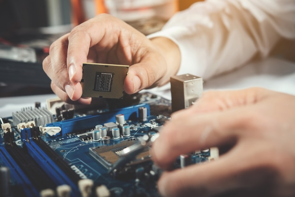
Automated Optical Inspection PCB(AOI) is a critical process in PCB manufacturing that involves the use of advanced imaging technology to inspect and detect defects on printed circuit boards. With the increasing complexity and miniaturization of PCBs, manual inspection methods are no longer sufficient to ensure the quality and reliability of electronic products. Maker-ray‘s AOI plays a crucial role in quality control, enabling manufacturers to identify and rectify defects early in the production process, saving time and resources.
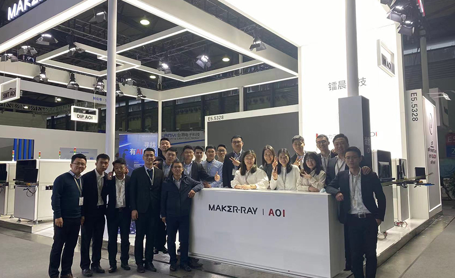
Advantages of Maker-ray Automated Optical Inspection PCB Systems
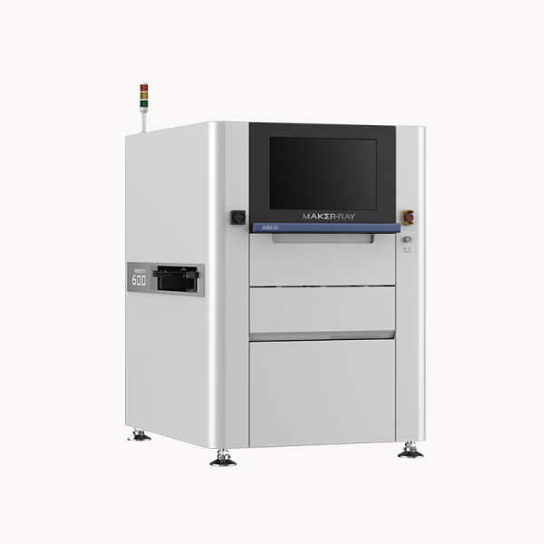
Maker-ray offering advanced features and capabilities that enhance the inspection process. Our systems utilize high-resolution cameras, sophisticated algorithms, and machine learning techniques to achieve accurate and reliable defect detection. Maker-ray AOI systems are designed to handle the intricacies of modern PCBs, including complex component placements, fine-pitch soldering, and multi-layer boards. With our state-of-the-art technology, Maker-ray ensures that even the smallest defects are detected, ensuring optimal product quality.
Furthermore, Maker-ray AOI systems offer enhanced speed in defect detection, significantly reducing inspection time compared to manual methods. This increased efficiency allows for faster production cycles and shorter time-to-market for electronic products. Additionally, by automating the inspection process, Maker-ray minimizes human errors and inconsistencies, improving overall productivity and reducing the need for rework or repair.
Impact of Automated Optical Inspection on PCB Manufacturing
The adoption of automated optical inspection PCB has a profound impact on PCB manufacturing processes and outcomes. By ensuring the detection and elimination of defects early in the production cycle, AOI contributes to improved product quality and reliability. Defects such as solder bridges, missing components, misalignments, and solder joint issues can be swiftly identified and rectified, preventing costly failures and repairs down the line. The use of Maker-ray AOI systems instills confidence in the quality of the produced PCBs, leading to enhanced customer satisfaction and a positive brand reputation.
Moreover, automated optical inspection PCB brings significant cost savings to PCB manufacturers. By detecting defects early, scrap and rework rates are reduced, minimizing material waste and production costs. The streamlined inspection process also eliminates the need for manual labor, freeing up resources and enabling manufacturers to allocate our workforce to more value-added tasks.
Conclusion
In conclusion, automated optical inspection PCB, particularly with Maker-ray’s advanced AOI systems, plays a vital role in PCB manufacturing. The benefits of AOI include enhanced accuracy and speed in defect detection, reduced human errors, improved product quality, cost savings, and increased customer satisfaction. By embracing automated optical inspection PCB, manufacturers can ensure the reliability and high-quality of our PCBs, ultimately contributing to our success in the competitive electronics industry.