In the world of PCB manufacturing, precise solder paste inspection is paramount. 3D SPI (Three-Dimensional Solder Paste Inspection) plays a crucial role in ensuring the quality and reliability of printed circuit boards. By accurately inspecting the solder paste deposition before reflow, 3D SPI helps manufacturers adhere to industry standards and specifications, preventing costly rework and reducing production delays. With Maker-rayhttps://maker-rayaoi.com/‘s cutting-edge 3D SPI technology, manufacturers can streamline our quality control processes and achieve consistent high-quality PCB assemblies.
Introducing Maker-ray’s Cutting-edge 3D SPI Solutions
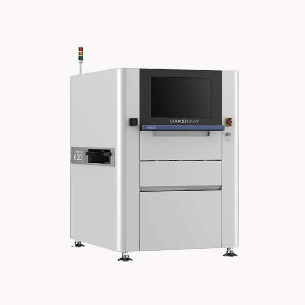
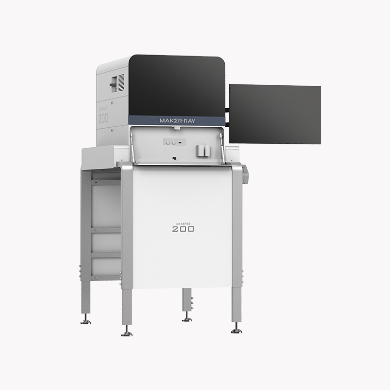
Maker-ray is a leading provider of advanced 3D SPI solutions designed to optimize PCB assembly quality control. Our state-of-the-art technology combines high-resolution imaging and accurate measurement capabilities to deliver precise inspection results. Our commitment to excellence and innovation has made Maker-ray a trusted name in the industry. We understand the critical importance of quality control in PCB assembly, and our advanced 3D SPI solutions are specifically engineered to meet the evolving demands of modern manufacturing processes.
At Maker-ray, we believe that precision is key when it comes to inspection and measurement. Our cutting-edge technology employs high-resolution imaging, allowing for detailed analysis of solder joints, component placement, and other critical features of the PCB. This level of accuracy ensures that even the smallest defects or inconsistencies are detected, enabling manufacturers to take proactive measures to rectify them.Maker-ray’s 3D SPI systems utilize advanced algorithms and artificial intelligence to intelligently detect defects, ensuring thorough analysis and reliable inspection outcomes. With Maker-ray’s solutions, manufacturers can benefit from robust and efficient PCB quality control.
Advantages of Maker-ray’s 3D SPI Solutions for Manufacturers
- Enhanced Process Efficiency and Reduced Production Costs:
By integrating Maker-ray’s 3D SPI solutions into our manufacturing processes, businesses can achieve enhanced process efficiency. The automated inspection process saves time and resources, reducing the need for manual inspections. This streamlined workflow leads to increased productivity and ultimately helps reduce production costs.
- Improved Quality Control and Reduced Defect Rates:
Maker-ray’s 3D SPI technology enables manufacturers to achieve superior quality control. With our high-resolution imaging and precise measurements, it accurately identifies solder paste defects such as insufficient or excess solder, bridging, and misalignment. By catching these issues early in the assembly process, manufacturers can minimize defect rates and deliver products of exceptional quality.
- Competitive Edge through Consistent High-Quality PCB Assemblies:
By leveraging Maker-ray’s 3D SPI solutions, manufacturers gain a competitive edge in the market. Consistently high-quality PCB assemblies build customer trust and loyalty, fostering a reputation for reliability and excellence. With Maker-ray’s technology, businesses can meet and exceed customer expectations, positioning themselves as industry leaders.
Conclusion
In conclusion, Maker-ray’s cutting-edge 3D SPI solutions provide manufacturers with the tools we need to streamline PCB quality control. By ensuring precise inspection, reducing production costs, improving quality control, and delivering consistent high-quality PCB assemblies, Maker-ray empowers businesses to thrive in the competitive PCB manufacturing landscape. With Maker-ray’s advanced technology at our disposal, manufacturers can confidently produce superior products and exceed customer expectations.