In the rapidly evolving landscape of electronics manufacturing, ensuring precise solder paste deposition is vital for optimal product performance. 3D Solder Paste Inspection (SPI) has emerged as a game-changing technology, enabling accurate and efficient inspection of solder paste quality. In this article, we explore the significance of 3D SPI and introduce Maker-ray, a leading provider in the field. We will also highlight the value of Maker-ray’s Field Application Engineer (FAE) service and training, empowering businesses to optimize the performance of their 3D SPI systems.

The Power of 3D SPI in Solder Paste Inspection
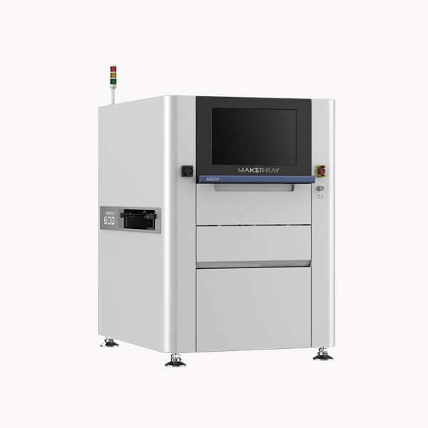
3D SPI technology has revolutionized solder paste inspection in electronics manufacturing. These advanced systems employ high-resolution cameras and laser profiling techniques to capture detailed images of solder paste deposits on printed circuit boards (pcbs). By analyzing the height, volume, and shape of the solder paste, 3D SPI systems ensure accurate inspection, detecting defects such as insufficient or excessive solder, bridging, and misalignment. With real-time feedback and data-driven insights, 3D SPI enables manufacturers to optimize their production processes, minimize rework, and enhance overall product quality.
Maker-ray Elevating 3D SPI Solutions
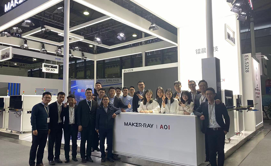
Maker-ray is a trusted industry leader, specializing in providing advanced 3D SPI systems that redefine solder paste inspection in electronics manufacturing. With deep expertise in machine vision and metrology, Maker-ray has developed cutting-edge solutions that deliver exceptional accuracy and reliability. The brand’s commitment to innovation, quality, and customer satisfaction has solidified its position as a preferred provider of state-of-the-art 3D SPI systems. Maker-ray empowers businesses to achieve superior solder paste inspection, streamline production processes, and drive operational excellence.
Leveraging Maker-ray’s FAE Service and Training for Optimum Performance
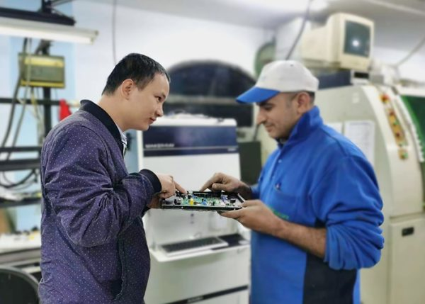
To help businesses maximize the potential of their 3D SPI systems, Maker-ray offers a comprehensive Field Application Engineer (FAE) service and training program. The FAE service provides expert guidance and support throughout the integration and implementation of Maker-ray’s 3D SPI systems. Maker-ray’s skilled Field Application Engineers possess extensive knowledge of the technology and can provide tailored solutions to meet specific customer requirements. We collaborate closely with clients to ensure seamless system integration, optimize performance, and address any challenges that may arise.
In addition to the FAE service, Maker-ray’s training program equips businesses with the necessary skills and proficiency to operate and maintain 3D SPI systems effectively. Through hands-on training sessions, interactive workshops, and educational resources, employees gain in-depth knowledge of 3D SPI technology, enabling them to harness the full potential of their systems. This knowledge transfer fosters self-sufficiency, reduces reliance on external support, and promotes continuous improvement in solder paste inspection practices.
Conclusion
3D SPI technology plays a crucial role in ensuring precise solder paste inspection in electronics manufacturing, and Maker-ray stands as a trusted provider of advanced solutions. With its FAE service and comprehensive training program, Maker-ray empowers businesses to optimize their solder paste inspection processes, improve product quality, and drive operational efficiency. By embracing Maker-ray’s FAE service and training, businesses can unlock the full potential of their 3D SPI systems, ensuring superior solder paste inspection, reducing errors, and gaining a competitive advantage in the industry.