Accurate solder paste inspection is crucial in the PCB manufacturing industry. Technology known as 3D SPI (Three-Dimensional Solder Paste Inspection) is essential for obtaining precise and trustworthy inspection findings. Maker-ray‘s 3D SPI assists manufacturers in upholding the highest standards for our PCB assemblies by guaranteeing adherence to industry standards and specifications. By identifying and resolving solder paste faults early in the manufacturing process, it also reduces rework and production delays.

The Advanced 3D SPI Solutions from Maker-ray
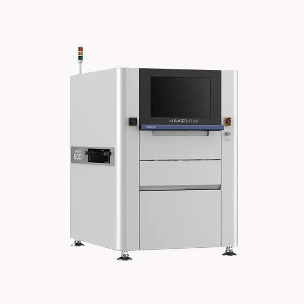
Maker-ray is a renowned provider of advanced 3D SPI solutions that are revolutionizing PCB manufacturing. Our cutting-edge technology offers a comprehensive approach to inspection. Maker-ray’s 3D SPI systems are equipped with high-resolution imaging and precise measurement capabilities, enabling manufacturers to capture detailed data on solder paste deposition. Moreover, Maker-ray integrates artificial intelligence into our solutions, enabling intelligent defect detection and analysis. This combination of advanced features ensures accurate and efficient inspection outcomes.
Key Benefits of Maker-ray’s 3D SPI Solutions
- Enhanced Process Efficiency and Reduced Costs:
Maker-ray’s 3D SPI solutions significantly enhance process efficiency in PCB manufacturing. The automated inspection process reduces the reliance on manual labor, saving time and resources. By streamlining the inspection workflow, manufacturers can optimize our production processes, resulting in reduced costs and increased overall efficiency.
- Improved Quality Control and Reduced Defect Rates:
With Maker-ray’s advanced 3D SPI technology, manufacturers can achieve improved quality control. The high-resolution imaging and precise measurement capabilities allow for thorough and accurate inspection of solder paste deposition. By identifying defects early in the manufacturing process, manufacturers can take corrective actions promptly, reducing defect rates and ensuring high-quality PCB assemblies.
- Streamlined Workflow and Increased Productivity:
Maker-ray’s 3D SPI solutions contribute to a streamlined workflow and increased productivity. The integration of advanced features and intelligent defect detection eliminates the need for manual inspections and reduces the chances of human error. This streamlined approach accelerates the manufacturing process, enabling manufacturers to meet deadlines and deliver high-quality products to our customers.
Conclusion
In conclusion, Maker-ray’s advanced 3D SPI solutions are transforming PCB manufacturing by enhancing efficiency, improving quality control, and streamlining workflows. By leveraging high-resolution imaging, precise measurements, and intelligent defect detection, Maker-ray enables manufacturers to achieve superior solder paste inspection results. Implementing Maker-ray’s 3D SPI technology optimizes production processes, reduces costs, and ensures high-quality PCB assemblies, making it a valuable investment for businesses seeking to enhance our manufacturing capabilities.